
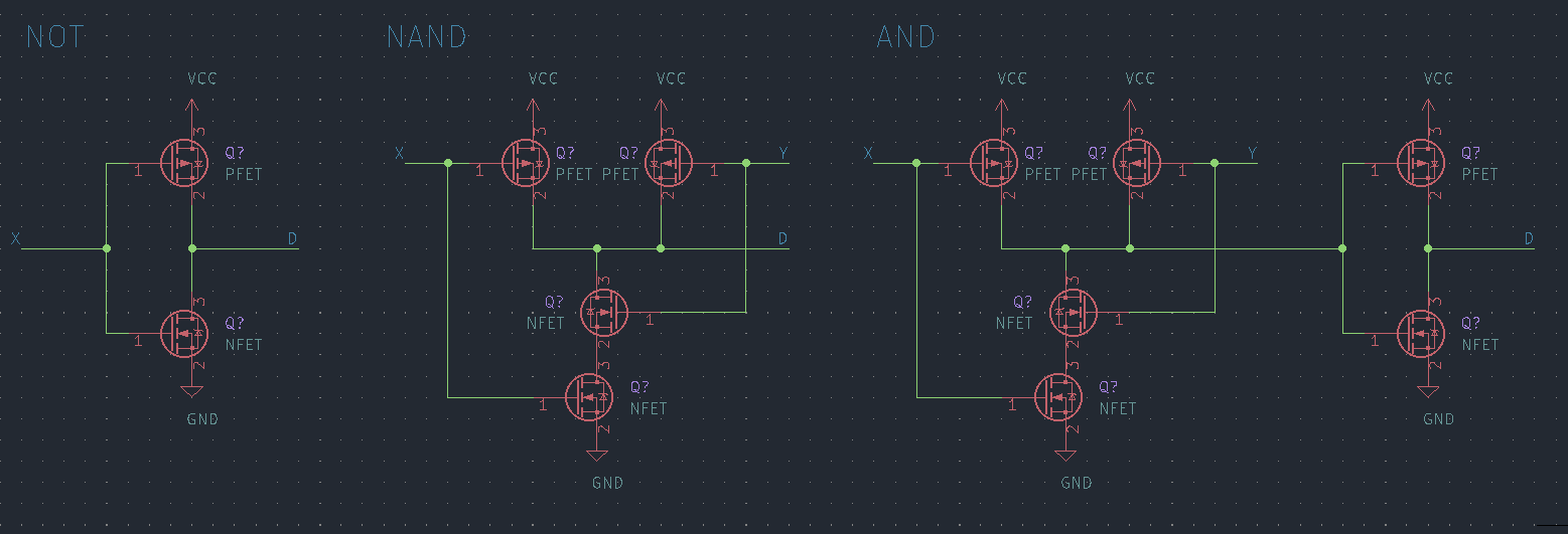
whack how the standard implementation of an AND gate is actually a NAND gate tied into a NOT gate
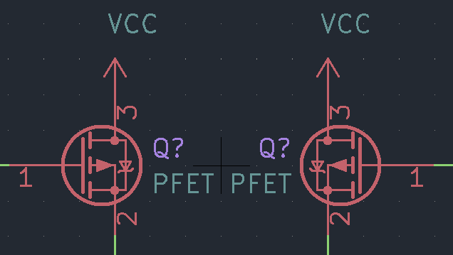
so the most annoying thing putting this into an educational + aesthetic pcb form is that to make the schematics pretty you mirror the mosfet symbols, but you can't do that with real ones unless you find ones with different pinout (oh and added issue, the most common pinout has gate, source on one side and drain on the other, mismatch with the common directions the pins point in symbol-wise)
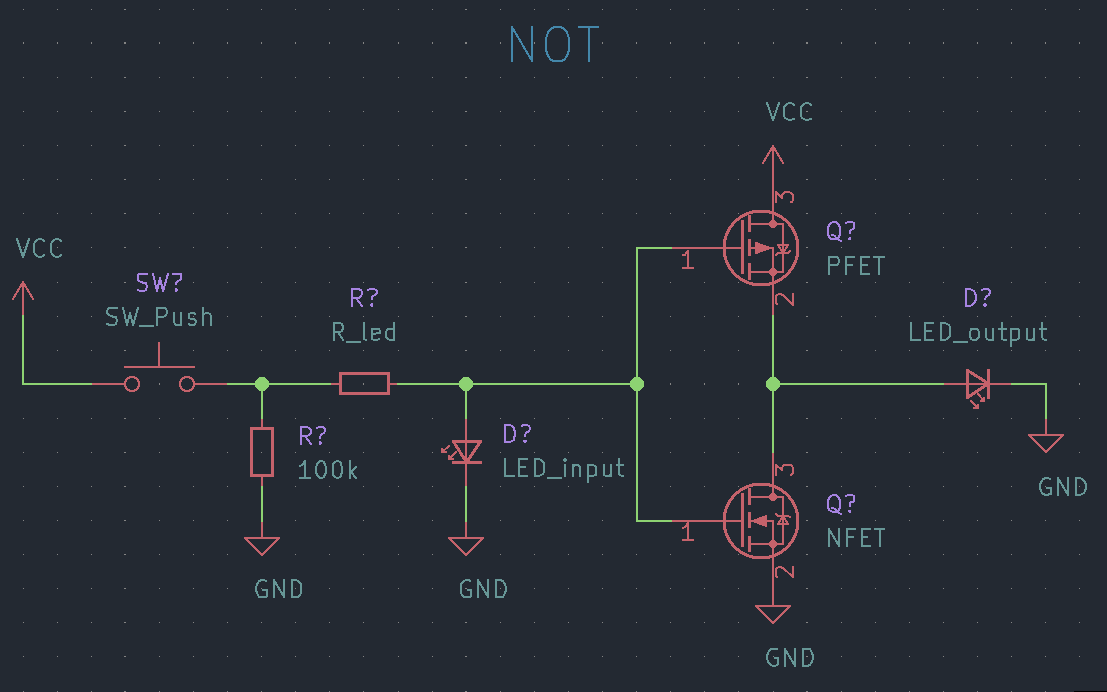
i have no clue if this will actually work out, but it should be a good way to get an input from button, visualized with 1 led (blue), with output visualized by another (green)
i'd basically be turning https://www.youtube.com/watch?v=QZwneRb-zqA into pcb form, section by section

so i'll have to experiment with a schematic footprint that doesn't care about the actual transistor's orientation, but draws silkscreen around it to describe the schema behind it